


 , Nadjette Hamani 1, Abdallah Attaf 1, Nadia Lehraki 1, Ouanassa Haif Khaif 1, Malika Nouadji 1, Brahim Gasmi 1
1 Physics Laboratory of Thin Layers and Applications, University of Biskra, 07000 Biskra, Algeria
Abstract
This study investigates the influence of cation (Cu2+) and anion (Br-) doping on the physical properties of indium oxide thin films to evaluate their potential for transparent conductive oxide (TCO) applications. Undoped, Cu2+-doped, and Br--doped indium oxide thin films were grown on glass substrates (sample size: 1.25 cm × 1 cm) using the ultrasonic spray pyrolysis technique, and their structural, optical, and electrical characteristics were investigated using X-ray diffraction (XRD), ultraviolet-visible spectroscopy (UV-Vis), and the four-point probe technique. XRD revealed that Cu2+ doping reduced the average crystallite size, whereas Br- doping had little effect. Optical characterization indicated that Br doping enhanced their transmittance to 85%, with a slight widening of the bandgap from 3.69 to 3.73 eV, while Cu2+ narrowed it to 3.66 eV. Electrical measurements revealed that Br- incorporation reduced resistivity and yielded a superior figure of merit. The study concludes that bromine doping significantly improves the optoelectronic performance of In2O3 films compared to copper doping, suggesting that Br-doped films are promising candidates for high-performance transparent conductive electrode applications.
Keywords
- indium oxide thin films
- copper doping
- bromine doping
- ultrasonic spray pyrolysis
- transparent conductive oxide
Indium oxide (In2O3) is recognized as a wide-bandgap semiconductor, with a direct gap reported around 3.6 eV [1]. This material has been extensively studied both in fundamental research point of view and as a platform for practical device applications [2]. Due to its high optical transparency and inherent n-type conductivity, In2O3 serves as a key component in liquid crystal displays, light-emitting diodes, and photovoltaic cells, where transparent contacts are required [3, 4, 5]. Beyond these uses, it has been applied in gas sensing and biosensing [6], as well as in energy-related technologies such as photocatalysis and photoelectrochemical conversion [7], in addition to ultraviolet photodetection [8]. Among several preparation techniques, spray pyrolysis is considered particularly attractive for its straightforward operation, low cost, and ability to coat large surfaces effectively [9].
The electrical and optoelectronic behavior of In2O3 thin films is largely dictated by intrinsic point defects, particularly oxygen vacancies and interstitials [10, 11], and it can be controlled by conditions used during deposition and subsequent treatments [12]. Introducing extrinsic dopants offers a well-established route to adjust carrier concentration, mobility, and optical transparency, thereby allowing precise control over both conductivity and light transmission [10]. In the bixbyite lattice, indium ions (In3+) occupy the cationic positions, while oxygen ions (O2-) are situated at anionic sites. Incorporation of dopants usually takes place through substitution at these sites, provided that the ionic radius and charge state of the dopant are compatible with those of the host matrix [13]. Numerous investigations [14, 15, 16, 17] have demonstrated that doping In2O3 with transition- and post-transition-metal cations can markedly alter its electrical and optical properties, primarily through mechanisms involving lattice strain, defect state creation, and charge-compensation effects [18]. In particular, copper incorporation, typically explored in the form of ultrathin interlayers combined with established transparent conducting oxides (TCOs), has demonstrated the performance improvement of GaN-based optoelectronic devices by facilitating carrier injection and improving light extraction [19, 20, 21]. However, studies on Cu-doped In2O3 thin films prepared by spray pyrolysis as independent TCOs remain rare, leaving open questions regarding their structural, optical, morphological and electrical characteristics.
Anion doping offers another route to modulate the functionality of In2O3. Substituting oxygen with halide ions such as F–, Cl–, or Br– can lead to lattice expansion, band-structure modification, and altered defect equilibria, thereby influencing both conductivity and transparency [22, 23, 24, 25]. Among halogens, bromine is considered chemically stable under certain processing conditions but has received comparatively little attention. Only a few studies have examined Br-doped In2O3, particularly with respect to its structural and optoelectronic characteristics, which is the motivation of the present investigation.
In this work, we investigate the influence of cationic (Cu2+) and anionic (Br–) elements on the structural, optical, morphological, and electrical characteristics of In2O3 thin films deposited by spray pyrolysis. We place particular focus on the comparison between the distinct effects of these dopants and their importance for optimizing the performance of In2O3-based transparent conductive films.
Undoped and doped In2O3 thin films were deposited on glass substrates
(sample size: 1.25 cm
The structural characteristics of the IO, CIO, and BIO films were investigated by X-ray diffraction (XRD, X’Pert PRO, PANalytical, Almelo, The Netherlands). The thickness of the films, as determined by the gravimetric method, ranged from 460.00 to 620.00 nm. Surface morphology was assessed using a scanning electron microscope (SEM, Prisma E, Thermo Fisher Scientific, Waltham, MA, USA). Optical transmittance and absorption spectra were recorded with a ultraviolet-visible spectroscopy (UV-Vis, Lambda 950, PerkinElmer, Waltham, MA, USA). Electrical measurements, including sheet resistance determination, were carried out using the standard four-point probe method.
The XRD patterns shown in Fig. 1 correspond to the IO, CIO, and BIO films. Identified peaks match with the (211), (222), (400), (411), (440), (600), and (611) planes, consistent with the cubic In2O3 structure (JCPDS 06-0416). All samples display a dominant (400) diffraction peak. XRD does not reveal any secondary crystalline phases across all studied samples. Additionally, a suppression of non-primary peaks is observed, particularly in the CIO sample.
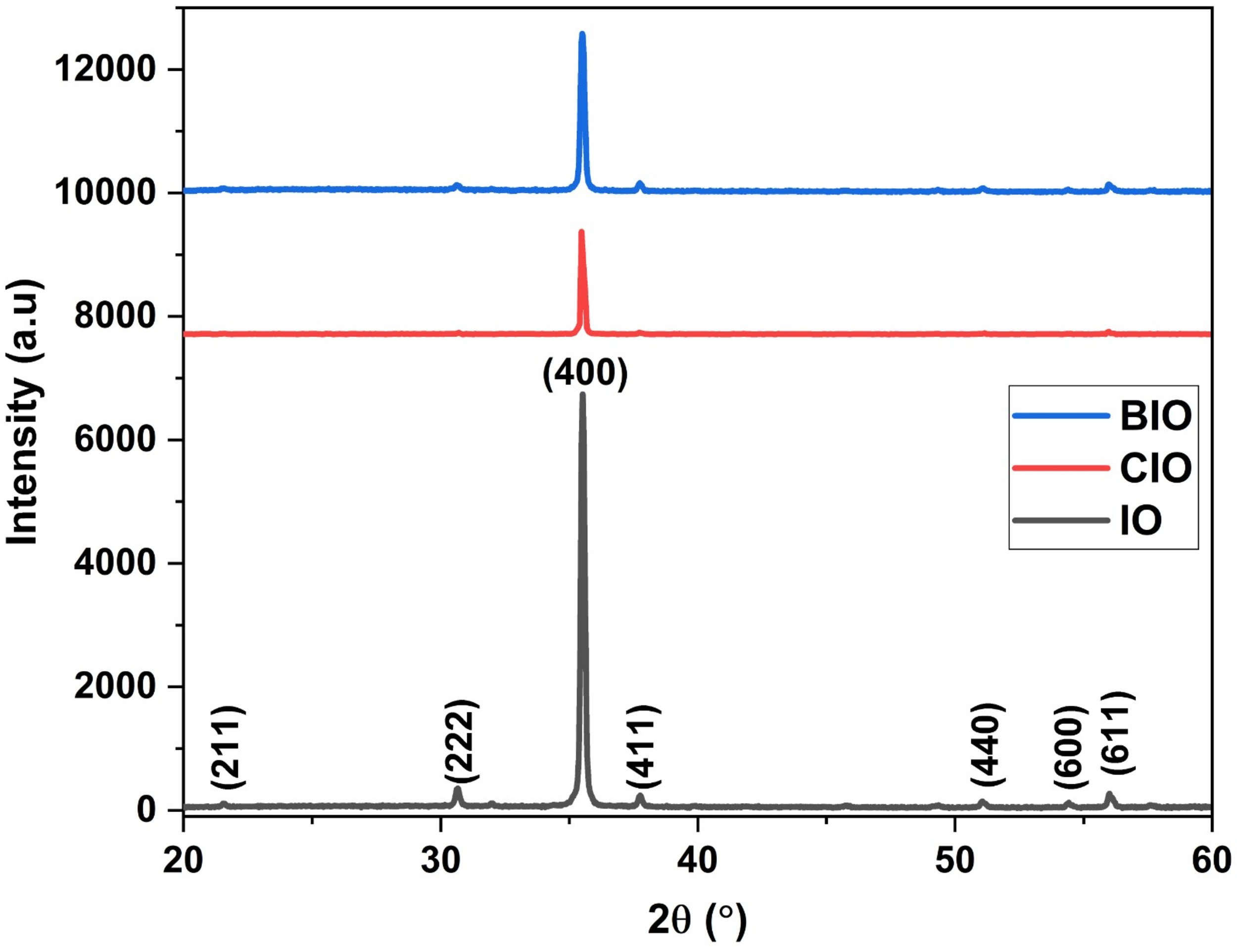 Fig. 1.
XRD patterns of the synthesized thin films. The plot displays
the diffraction intensity versus 2
The lattice constant (a) of the cubic In2O3 was determined using the following relation:
Where d denotes the interplanar spacing and h, k, l are the Miller indices. The calculated d values, lattice constants, and the positions of the (400) diffraction peak are summarized in Table 1. For the IO sample, the peak is located at 35.5018°. In the BIO sample, the peak position is found at 35.4694°, while for the CIO sample, it is recorded at 35.5336°. The determined lattice constants (a) are 10.106 Å for IO, 10.115 Å for BIO, and 10.097 Å for CIO.
| Samples | 2 |
d (Å) | Lattice constant a (Å) | Crystallite size D (nm) | Strain |
| IO | 35.5018 | 2.5266 | 10.106 | 44.269 | –0.0011 |
| CIO | 35.5336 | 2.5244 | 10.097 | 42.173 | –0.0020 |
| BIO | 35.4694 | 2.5288 | 10.115 | 44.220 | –0.0002 |
The crystallite size (D) and strain (
Where D represents the crystallite size,
According to the biaxial strain model [27, 28], the strain is defined as:
Where a is the calculated lattice constant and a0 is the standard value (10.118 Å) [29]. All prepared films exhibit negative strain values, as summarized in Table 1.
Fig. 2 presents representative SEM micrographs of the prepared In2O3-based thin films (Fig. 2a–c). Incorporation of Cu and Br dopants noticeably modifies the surface topography, resulting in distinct changes in grain morphology characterized by pyramidal and granular features. The BIO sample (Fig. 2c) exhibits densely packed grains. Furthermore, based on the SEM micrographs, the IO and BIO films appear more uniform, with a smoother surface texture than the CIO sample.
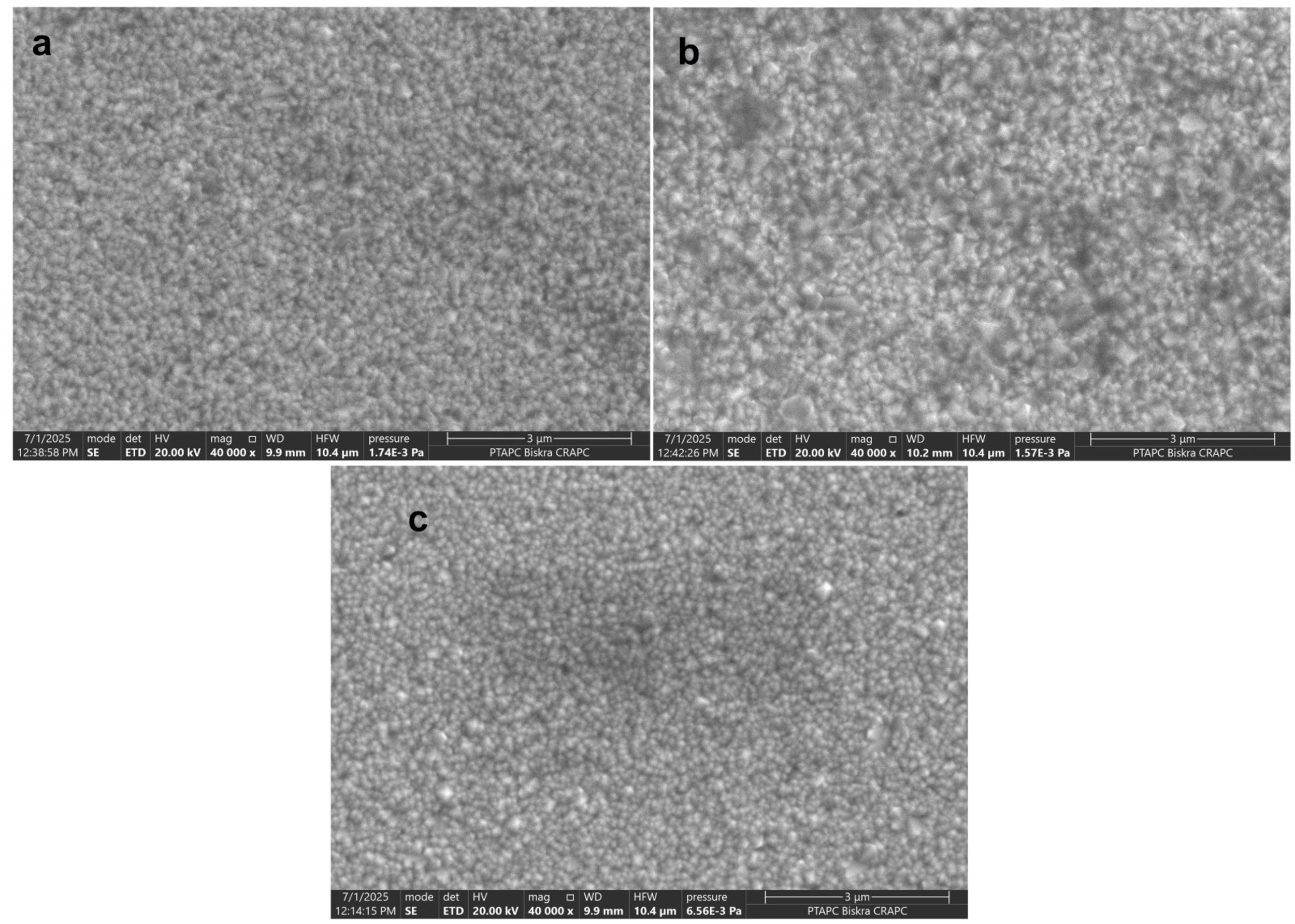 Fig. 2.
SEM micrographs illustrating the surface morphology of the prepared thin films. (a) IO, (b) CIO, and (c) BIO. The images reveal a significant influence of the dopant type on the grain size and surface topography. The IO film exhibits a dense distribution of crystalline grains, whereas Cu doping induces a modification in grain boundaries and surface roughness. In contrast, Br incorporation results in a comparatively smoother surface with a more uniform grain distribution, which correlates with the improved optical transparency discussed in the text. All images were captured at the same magnification to facilitate a direct comparison of the structural features. SEM, scanning electron microscope. Scale bar = 3 μm.
Fig. 3 presents the transmittance spectra of the IO, CIO, and BIO thin films. All films show high transparency across the visible region, with the BIO sample achieving the highest average transmittance of about 85%. A slight shift in the absorption edge toward the ultraviolet region is observed for the BIO film, while a shift toward the visible region is noted for the CIO film.
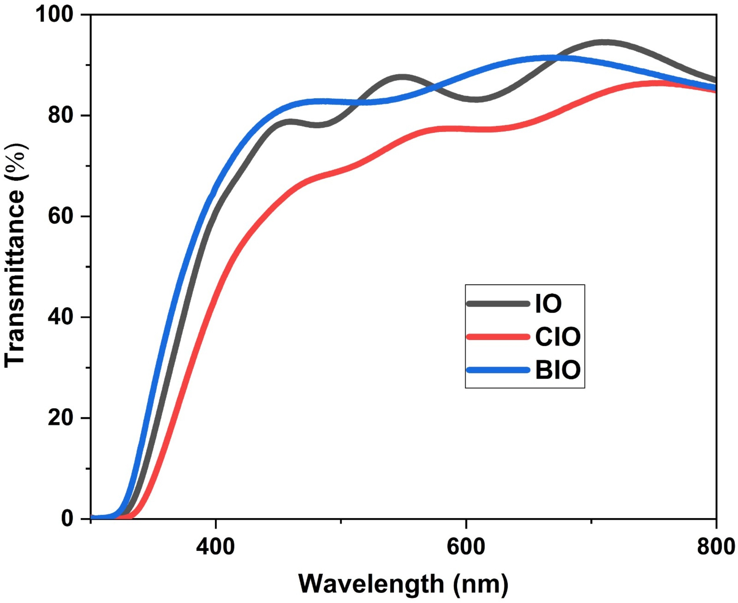 Fig. 3.
Optical transmittance spectra of IO, CIO, and BIO thin films recorded in the wavelength range of 300–1100 nm. The spectra reveal high transparency for all samples within the visible region, with the BIO film exhibiting the maximum average transmittance of approximately 85%. The variations in the absorption edge positions reflect the influence of copper and bromine incorporation on the electronic band structure. The enhanced transparency in the BIO sample is attributed to its improved crystalline quality and smoother surface morphology, which minimizes light scattering effects.
The optical absorption coefficient (
Where t represents the thickness of the thin film. To determine the
optical bandgap (Eg), Tauc’s plot was utilized by plotting
(
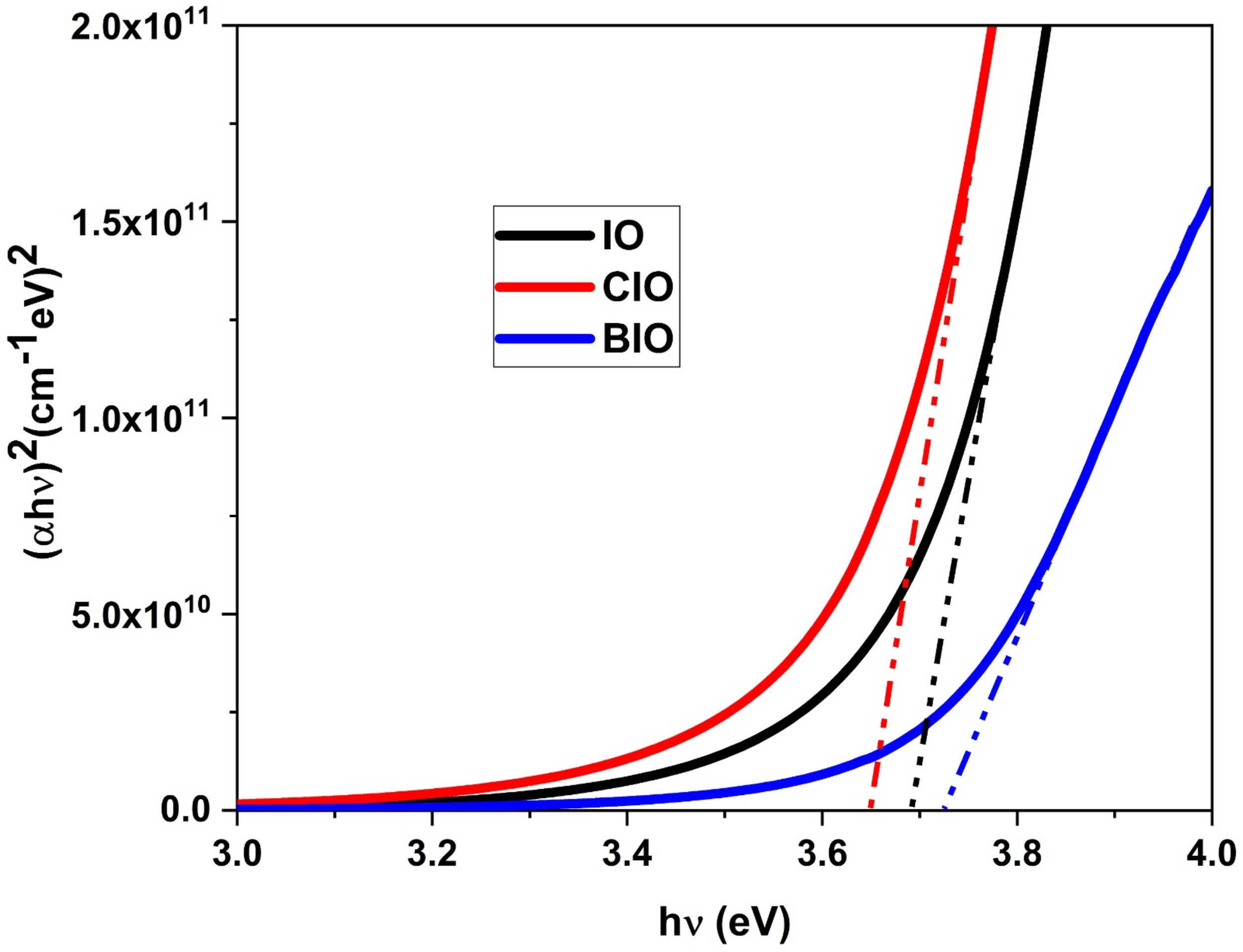 Fig. 4.
Tauc plots of (
The values of Eg were extracted by extrapolating the linear
portion of the curves to the photon energy axis where
(
Where A is a material-dependent constant and h is Planck’s constant. The calculated optical bandgap values for the IO, CIO, and BIO thin films are summarized in Table 2. The IO film exhibits an optical bandgap of approximately 3.69 eV, while doping with copper results in a slight reduction to 3.66 eV, and bromine incorporation increases the bandgap to around 3.73 eV.
| Samples | Eg (eV) | Eu (eV) | Tavg (%) (400–800 nm) | Resistivity ( |
T550 | Rsh ( |
Thickness (nm) | |
| IO | 3.69 | 0.332 | 84.78 | 0.0089 | 87.76 | 191.3978 | 14.159 | 460.00 |
| CIO | 3.66 | 0.343 | 75.04 | 0.0130 | 75.35 | 209.6098 | 2.815 | 620.20 |
| BIO | 3.73 | 0.329 | 85.38 | 0.0060 | 83.93 | 119.9904 | 14.455 | 500.04 |
Eg, optical bandgap energy; Rsh, sheet resistance; Eu, Urbach energy; Tavg, average transmittance; T550, transmittance at 550 nm.
The Urbach energy (Eu) was determined by following the empirical Urbach rule [31], which describes the exponential dependence of the absorption coefficient on photon energy near the band edge.
Where
Sheet resistance (Rsh) is commonly determined using the linear four-point probe method, in which a constant current (I) is passed through the two outer probes while the voltage drop (V) is measured between the inner probes. This setup significantly reduces the influence of contact and spreading resistance, enabling a more precise evaluation of sheet resistance. For thin films with a thickness (t) much smaller than the probe spacing, a geometric correction factor is applied, and the sheet resistance is estimated as follows:
The electrical resistivity (
As summarized in Table 2, the IO film exhibits a resistivity of 0.0089
To compare the performance of such films, the study uses the figure of merit
(
Where
Regarding the structural analysis, the dominance of the (400) diffraction peak observed in the XRD patterns (Fig. 1) indicates that this plane is the favorable growth direction due to its low surface energy and the high degree of crystallinity supported by it. This trend aligns with prior results reported by Bagheri Khatibani et al. [33] for films produced via spray pyrolysis. The preferred orientation remains unaffected by the incorporation of copper or bromine dopants. Ionic radius considerations suggest that Br– (1.96 Å), being larger than O2- (1.40 Å), may substitute anion sites, while Cu2+ (0.73 Å), slightly smaller than In3+ (0.80 Å), may replace cationic positions in the lattice.
Although no secondary phases were detected, amorphous phases or nanoscale Cu/Br-related precipitates below the technique’s detection limit cannot be fully ruled out. The suppression of non-primary peaks, especially in the CIO sample, indicates a reinforced preferential orientation in all films. Nevertheless, direct confirmation of dopant site occupancy and chemical state requires complementary techniques beyond XRD.
Regarding the lattice parameters, the shift of the (400) diffraction peak toward lower diffraction angles in the BIO sample suggests a small expansion in the interplanar distance. This change may be attributed to the possible substitution of O2- in the lattice by Br– of a larger ionic radius. In contrast, the shift of the (400) peak toward higher diffraction angles for the CIO sample is indicative of a contracted interplanar spacing, which is consistent with the possible replacement of In3+ by smaller Cu2+ ions [34]. These trends are supported by ionic radius considerations and align with findings in the literature [35].
The observed reduction in crystallite size upon doping is particularly
pronounced with copper incorporation compared to the almost negligible decrease
induced by bromine (see Table 1). This behavior is consistent with reports
regarding the influence of dopants on the nucleation and growth of
In2O3 thin films [36]. Furthermore, the negative
In addition to the structural changes, the surface morphology of the films was also significantly affected by the dopant type. These morphological observations are consistent with earlier reports showing that grain structure in In2O3 films is highly dependent on deposition conditions [37]. Although the present SEM discussion is qualitative, such variations in grain geometry and packing density are significant as they may influence the optical and electrical properties of the films by affecting light scattering, charge transport pathways, and surface state density [38].
Consistent with the transmittance spectra shown in Fig. 3, the improvement in optical transmission observed in the BIO sample is possibly linked to a reduction in light scattering and enhancement in crystalline quality. In particular, the greater transparency observed in the IO and BIO films may be associated with their comparatively smoother surface morphology, which helps to suppress scattering effects at the film surface. This relationship is consistent with the SEM observations discussed in the previous section. It is well established that increasing the surface roughness leads to greater light diffusion and consequently lowers transmittance. Previous work confirms that rougher surfaces increase light diffusion, thereby degrading transmittance [39].
As evidenced by the optical data presented in Section 3.3, the optical bandgap of the IO film aligns well with previously reported values for In2O3 prepared via different synthesis methods [40, 41]. The observed trends of bandgap narrowing in Cu-doped In2O3 and widening in Br-doped In2O3 are consistent with comparable results found in the literature for Cu and F doping [22, 42, 43]. Among the studied samples, the CIO film exhibits the lowest bandgap (3.66 eV) accompanied by an increase in Urbach energy (0.343 eV), which may be attributed to structural disorder and localized states that reduce the effective bandgap [44]. This is consistent with findings reported in the literature [45].
In contrast, bromine incorporation into indium oxide thin films leads to an optical bandgap enlargement and a reduction in Urbach energy. The shift of the absorption edge toward shorter wavelengths is consistent with a Burstein–Moss effect, whereby an increase in carrier concentration raises the Fermi level and shifts the onset of interband transitions. The lower Urbach energy indicates a reduction in disorder-induced tail states near the band edges. Collectively, these trends suggest that Br doping enhances the optical transparency window of In2O3 films [23]. The tunable bandgap indicates that doped In2O3 films can offer tailored optical properties for transparent conductive applications.
Consistent with the data presented in Section 3.4, the electrical resistivity of In2O3 thin films is strongly influenced by the dopant species and the resulting defect chemistry. The intrinsic n-type behavior of the IO film is primarily due to the presence of oxygen vacancies (V0) and interstitial indium atoms (Inᵢ), both of which act as shallow donor states [46, 47]. The increase in resistivity observed in the CIO film may be related to the substitution of indium sites by copper atoms, where they act as acceptor impurities. These acceptor levels introduce holes that compensate conduction-band electrons, thereby reducing the free carrier concentration and increasing the film’s resistivity [48].
In contrast, the reduction in resistivity for the BIO film is consistent with the possible substitution of O2- in the lattice by Br–, which may introduce shallow donor levels. These defects may increase the electron density in the conduction band without a substantial increase in ionized impurity scattering, resulting in enhanced conductivity.
The observed enhancement in electrical conductivity for the BIO sample, combined
with its high optical transparency, directly influences its overall performance
as a transparent conductor. Consequently, the BIO sample achieves the highest
figure of merit (
This work compares Cu- and Br-doped In2O3 thin films deposited by spray pyrolysis at a single dopant loading (4 wt.%) and one deposition temperature; thus, broader optimization is still required. Future studies should include dopant concentration series and Hall effect measurements to establish concentration–property trends and to separate carrier concentration from mobility effects. Dopant incorporation is inferred mainly from XRD; compositional/chemical-state analysis (e.g., EDS mapping, XPS, and/or SIMS) is needed for direct confirmation, while crystallite sizes from Debye–Scherrer remain approximate without microstrain/instrumental-broadening deconvolution (e.g., Williamson–Hall or Rietveld refinement). Finally, long-term stability and device-level validation were beyond the scope of this study and should be addressed using simple prototype demonstrators and stability testing.
In this work, undoped In2O3, Cu-doped In2O3, and Br-doped
In2O3 thin films were successfully deposited on glass substrates via
spray pyrolysis at 450 °C. XRD indicated that all films were
polycrystalline with a preferred orientation along the (400) plane. Incorporation
of Cu2+ slightly reduced the crystallite size from 44.3 to 42.2 nm, while
Br– doping produced little change in the crystallite size. The optical
bandgap of undoped In2O3 (3.69 eV) decreased modestly to 3.66 eV with
Cu2+, whereas Br– doping increased it to 3.73 eV, demonstrating the
possible fine-tuning of the film’s electronic structure. Electrical
characterization further showed that bromine doping lowered resistivity to around
6
The datasets used and analyzed during the current study are available from the corresponding author on reasonable request.
KB and NH conceived and designed the research study. KB, NH and NL performed the experimental work and sample preparation. OHK, MN and BG carried out the data acquisition and performed the XRD and UV-Vis characterizations. AA and KB analyzed and interpreted the data. KB and NH drafted the original manuscript. NL, OHK, MN, BG, and AA critically revised the manuscript for important intellectual content. All authors read and approved the final manuscript. All authors have participated sufficiently in the work and agreed to be accountable for all aspects of the work.
Not applicable.
The authors would like to thank all individuals who provided support during the preparation of this manuscript. The authors also appreciate the valuable comments and suggestions from the reviewers, which helped improve the quality of this work.
This research received no external funding.
The authors declare no conflict of interest.
During the preparation of this manuscript, the authors used AI-based tools (Gemini by Google and Grammarly) solely for language polishing and grammar checking. The authors reviewed and edited the content as needed and take full responsibility for the content of the publication.
References
Publisher’s Note: IMR Press stays neutral with regard to jurisdictional claims in published maps and institutional affiliations.